Mechanical stress can be present in coated optical components and be responsible for degraded performance or physical failure as a function of environmental conditions such as temperature excursions. Stress effects are of high concern for coating optics that cycle to and operate at cryogenic temperatures, a requirement for many IR systems.
Left unmanaged, stress in thin films can degrade optical function, cause delamination, and shorten device lifespan in exactly the environments where sensors need to perform most. Understanding stress causes and how to control them is important for specifying, manufacturing, and operating a precision coating system.
Origins of Mechanical Stress in Thin Films
Total accumulated stress magnitude results from a complex interrelation of film composition, deposited layer growth structure, thermal expansion coefficients, and substrate adhesion forces, as well as externally applied forces. Researchers differentiate between intrinsic and extrinsic strains that produce stress.
Intrinsic stresses are caused by internal strains within the film layer that result from non-amorphous structure, such as columnar and void micro-structure. Different layer materials in a multi-layer design will have different magnitudes and directions of strain. Compressive and tensive stress can be presented by different materials in a multi-layer. The total stress contributed is proportional to the layer thickness and thus to total coating physical thickness.
Extrinsic stress is imposed by thermal expansion differences between layer materials and the substrate material. External conditions, such as temperature excursions, especially to low temperatures, cause high strains. Temperature departures from the deposition temperature can result in cracking, delamination, and threaten adhesion.

Both types create problems. Compressive stress can cause film buckling. Tensile stress beyond a critical threshold leads to cracking or delamination. For thermal imaging applications, even minor delamination or micro-cracking can scatter infrared radiation and destroy detector performance. The coating designer will attempt to balance compressive and tensive stress to minimize total accumulated stress. The approach will consider coating design, layer materials, substrate composition and deposition process.
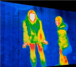
Why Thermal Imaging Sensors Are Particularly Vulnerable
Semiconductor thermal imaging sensors often require cooling to LN2 or lower temperatures. The associated filters and AR coatings are also cooled. Even uncooled microbolometers that have extremely thin, mechanically fragile membranes are subject to stress-induced damage. These membranes must be thermally isolated to detect subtle infrared signals. The challenge is that the films deposited on these membranes, including sensing layers like vanadium oxide and absorber stacks, are highly sensitive to the effects of residual stress.
Stress becomes even more critical when sensors are deployed in aerospace and defense environments. Temperature swings between ground and altitude, combined with vibration and shock loading, apply cyclic mechanical demands to coated assemblies. A film may survive lab qualification but still fail in the field if engineers did not properly manage its stress state during deposition.
Key failure modes linked to film stress in thermal imaging applications include:
- Crazing and microcracking of the coating resulting in scatter and altered spectral properties
- Catastrophic delamination at interlayer and substrate interfaces, particularly on germanium (Ge) or zinc selenide (ZnSe) optics, where adhesion is already weak
- Optic Deformation changes the optical performance
Deposition Process Variables That Drive Stress
Deposition process parameters, such material kinetic energy, ion assist energy, deposition rate, partial pressures, and substrate temperature have large influences on film stress generation because they determine micro-structure and composition of the deposited layer. These variables interact. A small change in one can shift a film from tensile to compressive, or vice versa.
Ion-assisted deposition is one of the most effective tools for controlling stress. When energetic ions bombard the growing film, they transfer kinetic energy to adatoms. This additional energy allows atoms to settle into denser, more stable configurations. Low ion energies, approximately 100 eV or less, tensile stress in vapor-deposited metal films can be reduced without driving the film toward problematic compression.
Plasma-assisted processes offer a related mechanism. High-density plasma sources increase adatom mobility energy without requiring elevated substrate temperatures. This matters for heat-sensitive substrates. Plasma Assisted Deposition (PAD) decreases internal film stress. It also improves adhesion and film density, compared to conventional electron beam evaporation alone.

Process variables worth monitoring and controlling for stress management include:
- Ion energy and ion-to-atom arrival ratio during ion-assisted evaporation or IBS processes
- Substrate temperature maximum and uniformity across the fixture during deposition
- Deposition rate, which affects adatom diffusion time and packing density
Working pressure for sputter-based processes, since higher pressures increase the mean free path and reduce ion energy at the substrate, stress can be modified.
Matching the Process to the Sensor Substrate
Substrate selection drives much of the stress management strategy. Germanium, silicon, ZnS, and ZnSe all have distinct coefficients of thermal expansion and surface chemistry. Often, a binding or adhesion layer must be added between the substrate and the functional film stack to counteract interfacial stress and prevent delamination.
For temperature-sensitive substrates, including polymer optics and certain focal plane array assemblies, low-temperature deposition methods are a requirement rather than an option. Cold plasma approaches enable film formation at temperatures below 100°C. This removes the thermal mismatch stress that would otherwise develop when a hot film cools against a polymer substrate with a very different (high) thermal expansion coefficient.
Chamber design also plays a critical role. Fixturing geometry, substrate rotation strategy, and radiative heat management all affect how uniformly temperature distributes across the part during deposition. Non-uniform heating creates non-uniform stress gradients that are difficult to predict and difficult to correct after the fact.
Build It Right from the Start
If your process relies on thin films for temperature-challenging environments, thermal IR imaging sensors, engineers cannot treat stress management as an afterthought. They need to engineer it into the system from day one. In addition to coating stress management at the design stage, a deposition platform with process control of ion energy, plasma density, rate, pressure, and substrate temperature is essential.
Tecport Optics designs vacuum coating systems with exactly this kind of process control. Our Plasma Assisted Deposition systems and ion-assisted capabilities target the specific process variables that govern film stress. We work with your substrate materials, layer architecture, and production targets to configure a system that delivers repeatable, low-stress films from the first production run.
Reach out to our engineering team to discuss how we can support your thermal imaging coating requirements.