The two dominant physical vapor deposition (PVD) processes are sputtering and evaporation. Each delivers distinct trade-offs in film quality, versatility, throughput, and system cost. For engineers and technical decision-makers working with optical coating applications, understanding these differences is essential to achieving the right performance outcome.
How Evaporation Works in Optical Coating
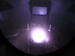
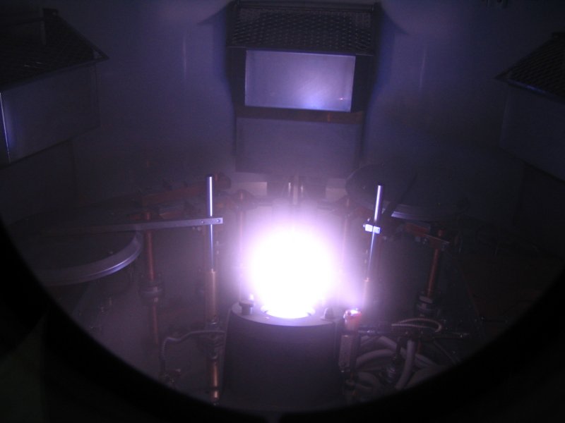
Evaporation is a thermal process. A source material is heated until it vaporizes, travels through a vacuum chamber, and condenses onto a substrate to form a thin film.
Two common variants are used in precision optics:
- Resistance-heated evaporation uses resistive heating elements for lower-melting-point materials
- Electron beam (e-beam) evaporation focuses a high-energy electron beam onto a target, enabling deposition of high-melting-point oxides and fluorides
Evaporation is widely valued for its high deposition rates and lower equipment costs. This makes it attractive for high-volume production runs. However, thermal evaporation is a low-energy process; consequently, film layers tend to have lower packing density and weaker substrate adhesion compared to sputtered films.
Sputtering, in contrast, offers superior film quality as evidenced by denser growth microstructure, better step coverage, and stronger adhesion due to the higher kinetic energy of the deposited particles. While sputtering equipment generally has a higher initial cost, its ability to deposit a wider variety of materials has specific advantages.
How Sputtering Works in Optical Coating
Sputter deposition is widely used in microelectronics, optics, and surface modification for creating thin films with precise composition and thickness. Sputtering is a kinetic process. High-energy ions bombard a solid target material, where they eject atoms from the surface. Those atoms then travel to and deposit on a substrate.
The target material is usually a pure element such as a metal, an alloy, or a compound. A plasma is created between the target and an anode in inert gas like Argon, and high-energy ions and sputtered atoms bombard the substrate.
Key forms of sputtering used in optical applications include:
- Magnetron sputtering uses a magnetic field to sustain the plasma, enabling faster deposition rates and larger area coverage. Some variations are DC and RF driven.
- Ion beam sputtering (IBS) delivers the highest film density, optimum optical quality including lowest absorption, setting the benchmark for laser optics and high-performance coatings.
Since the sputtering process is more energetic than evaporation, high substrate temperatures are not required, enabling its applicability to a wide range of substrates, including polymers.
Comparing Film Quality and Performance
Film quality is where the two methods diverge most sharply. Sputtered films are denser, more durable, and exhibit better adhesion to the substrate. IBS coatings in particular produce bulk-like film density, ultra-low absorption, and minimal scatter; all critical for high-power laser systems and defense optics.
Evaporated films, while excellent for many standard applications, are more porous in structure. This creates moisture sensitivity and wavelength shift over time. Ion-assisted deposition (IAD) is often added to e-beam evaporation systems to partially address this limitation by improving packing density during film growth.
Sputtered films also outperform evaporated films in laser-induced damage threshold (LIDT), environmental durability, and spectral stability. For aerospace and defense applications, these properties are non-negotiable.
When to Use Each Method
Neither approach is universally superior. The right choice depends on the application's specific requirements.
Evaporation is a strong fit when:
- High deposition rates and throughput are the priority.
- The substrate materials include compounds such as fluorides, sulfides, selenides, etc. used in IR coatings and low-temperature metals.
- Budget constraints favor lower equipment and operational costs
Sputtering is the better choice when:
- Materials include oxide and nitride compositions, and refractory compounds
- Low absorption, high reflectivity, and spectral precision are required
- The operating environment involves temperature cycling, humidity, and control of stress
- The application involves high-power or ultrafast laser coatings where high LIDT is critical
- Substrates are heat-sensitive, including polymers and certain composites.
For many production environments, both methods are used side-by-side. A facility may rely on e-beam evaporation for standard filter production and reserve IBS or PAD systems for high-specification defense and photonics components.
Build the Right System for Your Process
At Tecport Optics, we design and manufacture vacuum deposition systems built around your specific coating requirements. Whether you need a high-throughput evaporation platform or a high-performance sputtering system, our engineering team works directly with you to configure a solution that fits your process.
Our systems include plasma-assisted deposition (PAD) and ion beam sputtering (IBS) capabilities through our exclusive domestic partnership with Cutting Edge Coatings. We also offer e-beam evaporation platforms equipped with ion-assisted and plasma-assisted surface treatment options for maximum flexibility.
Reach out to us today if you're evaluating coating technology for a new production line. Let's find the right deposition approach for your application.