Laser induced damage (LID) from high-energy laser irradiance manifests in two distinct forms. Pulsed energy in the femtosecond frequency range creates explosive damage as the high energy concentrated in short pulses vaporizes a coating. These failures are associated with coating point defects. High fluences of longer CW, microsecond and nanosecond pulse width cause heating associated with absorption, and LID takes the form of thermal stressing that can cause cracking or delamination. It is the latter regime of LID in precision optics that we discuss here.
High-energy laser systems place severe thermal and mechanical demands on every optical surface along the beam path. For optical engineers building systems for aerospace, defense, and industrial applications, thermal stress represents a critical failure mode that compromises both system reliability and beam quality. Thin-film deposition processes can be engineered to control the magnitude of thermal load an assembly tolerates before experiencing optical distortion or physical destruction.
Managing these thermal dynamics requires a considered approach to substrate surface preparation, coating material selection, coating design, and thin-film deposition processes as we discuss below.
Mechanics of Laser-Induced Thermal Stress in Precision Optics
No dielectric coating achieves absolute transparency. Even ultra-low-loss thin-film stacks absorb a residual fraction of incident photons. At multi-kilowatt power levels, this minor absorption converts into localized heating within the dielectric layers.
Absorbed energy concentrates around microscopic structural defects, including voids, nodules, particulate inclusions, and residual moisture. Adding to heating by area absorption, defects form localized hot spots, establishing steep thermal gradients across the cold surrounding material. Differences in coefficients of thermal expansion (CTE) within a coating/substrate structure impose thermal-induced shear strain. When stresses exceed the cohesive and or adhesive strengths of the coating / substrate system, cracking, crazing or delamination can result.
Another potential effect of absorption-induced heating is thermal distortion of the optic. We discuss below approaches for achieving high laser-induced damage thresholds (LIDT).
Substrate Surface Quality as a Primary Thermal Defense
Achievement of high LIDT requires a smooth, defect-free surface on which the coating is grown. Standard polishing procedures frequently leave subsurface damage (SSD), and micro-roughness and fractures, which trap organic residue, slurry particles, and moisture. Under high-fluence exposure, these buried sites act as initiation points for laser irradiance-induced breakdown damage. Advanced substrate surface preparation mitigates these risks prior to entering the deposition chamber.
Established substrate surface preparation steps for high LIDT include:
- Superpolishing. Minimizes surface roughness below 1 Angstrom RMS while removing subsurface damage.
- Ultrasonic and Solvent Cleansing. Strips residual polishing compounds, hydrocarbon contaminants, and lipids from the surface.
- In-Situ Plasma Activation. Cleans and activates substrate surface bonds without introducing thermal shock, enhancing physical film adhesion.
- High-Vacuum Bake-Out. Drives off adsorbed atmospheric water molecules prior to initial layer deposition.
- Contamination-Controlled Handling. Utilizes cleanroom environments, specialized tooling, and validated storage protocols to prevent re-contamination.
Plasma activation warrants detailed consideration in high-power optics manufacturing. Cold plasma treatments increase interfacial energy, forming stronger chemical bonds between the first thin-film layer and the substrate. This enhanced interfacial strength resists the high shear stresses generated during non-uniform laser heating.
Coating Material Selection for High-Thermal-Load Applications
Material selection establishes the baseline thermal performance of precision optics. Beyond providing target refractive indices, optical design engineers must evaluate three material properties: bandgap energy, thermal conductivity, and coefficient of thermal expansion (CTE).
Wide bandgaps minimize intrinsic absorption at operational wavelengths, while high thermal conductivity facilitates rapid dissipation of localized heat away from high-fluence regions. Matching the CTE between alternating thin-film layers and the base substrate minimizes residual film stress under operational temperature swings.
When designing robust optical stacks, engineering guidelines recommend:
- Selecting Wide-Bandgap Oxides. Utilize silica (SiO₂ ), hafnia (H fO₂), alumina (AlO₂ O₃), and tantala (Ta₂O₅) for low absorption and high damage thresholds across visible and near-infrared spectral regions.
- Minimize thermally-induced strain. Attempt to balance compressive and tensile stresses through CTE matching within film layers and substrate.
Coating Design has a Strong Design on LIDT
The arrangement of layers, and their thickness affect the distribution of the electric field maxima within a multi-layer stack. The coating designer will avoid placing E-field maxima in the high-index layers. Layer and substrate interfaces are locations vulnerable to LID.
Impurities tend to accumulate at interfaces, and abrupt material and index transitions are also locations where high E-fields can produce damage. Grading interfaces is an established procedure for reducing effects that plague abrupt interfaces.
Deposition Process Control and Thin-Film Density
Material selection alone cannot guarantee high LIDT performance; deposition technique has a major influence. Process energy, pressure and deposition rate influence LIDT. For example, packing density governs the environmental stability and intrinsic absorption of precision optics. Low-density films contain microscopic voids that absorb ambient atmospheric moisture. Under high-power laser irradiation, trapped water rapidly heats, vaporizes, and induces delamination.
Energetic thin-film deposition technologies overcome low density limitations. Ion-Assisted Deposition (IAD) and Ion Beam Sputtering (IBS) transfer kinetic energy directly to the growing film, packing adatoms into dense, amorphous microstructures. IBS platforms deliver exceptional control over stoichiometry, film density, yielding ultra-low-absorption optical coatings making the technique ideal for high LIDT applications.
Process control involving co-deposition from two sources can be designed to smooth interface transitions.
Process uniformity across the clear aperture remains equally crucial. Even a sub-one-percent variation in film thickness alters the spectral response and local electric field intensity (E-field) distribution within the stack. Real-time broadband optical monitoring provides precise layer thickness control during deposition, delivering repeatable, auditable LIDT performance across production batches.
Advanced Thin-Film Engineering with Tecport Optics
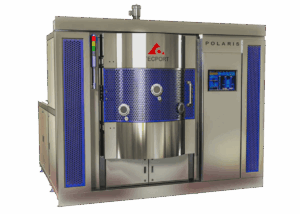
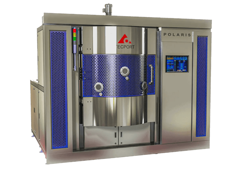
Tecport Optics can design, manufacture and deliver custom coating systems capable of producing specialized coatings with high LIDT.
Since 1997, Tecport Optics has engineered high-performance coating platforms configured around complex production needs. Our technology portfolio includes plasma-assisted deposition systems, PECVD, DLC, and state-of-the-art Ion Beam Sputtering solutions. By combining precise physical vapor deposition mechanics with robust process control, Tecport Optics empowers manufacturers to push the thermal boundaries of modern laser optics.
Optimize Your Optical Damage Thresholds
Thermal stress should not limit your optical system design or operational limits. Whether you require scalable production platforms or dedicated process development support to refine proprietary coating recipes, our engineering team brings decades of vacuum deposition expertise to your team.
Contact the technical specialists at Tecport Optics today to discuss your process requirements and discover how our custom thin-film deposition systems optimize high-power precision optics for demanding applications.
FAQs
Can you retrofit a standard PVD chamber to produce high-density films for high-power laser optics?
Facilities can upgrade existing chambers by adding an ion source, increasing high-vacuum pumping capacity, or modernizing automation controls to raise thin-film density significantly. This retrofit and component upgrade path usually costs far less than purchasing a new, full-scale deposition platform.
What is the proper method for cleaning high-power laser mirrors to prevent surface scratches and absorption sites?
Operators must use lint-free optical wipes with spectroscopic-grade solvents, applying a single-direction drag technique across the surface. You should never scrub the optic or reuse a dirty wipe, since improper cleaning creates microscopic scratches that later act as destructive absorption sites.
How does thin-film coating residual stress affect the surface figure and wavefront specifications of thin optical substrates?
High compressive or tensile stresses can measurably bend thin substrates, causing severe wavefront distortion. Thin-film designers mitigate this distortion by balancing opposing layer stresses across the multilayer stack or increasing the overall physical thickness of the substrate.